AIDL approach combines research and engineering centers, design center, growth and processing of high-quality crystals and a flexible production line for manufacturing chips for "systems-on-chip" and "systems-in-package".
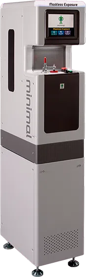
minimalFab is a complex of compact technological installations 30 centimeters wide that allow processing 0.5 inch diameter substrates and promptly producing various chips in small batches. Each technological process of chip manufacturing is implemented on a separate minimalFab installation. The time for substrate processing on one installation is not more than 60 seconds. The installations are connected to each other by a robot manipulator, which transports plates in hermetic containers "Minimal Shuttle". Minimal Shuttle eliminates the need to create "clean room" infrastructure, increases responsiveness and significantly reduces chip production costs.
The mobile laboratory-production complex AIDL VITIM allows producing microelectronic devices on Si, Ge, GaAs, SiN, SiC substrates using CMOS, MEMS, NEMS, VIS technologies and other new directions in electronic equipment development.